Affiliate links on Android Authority may earn us a commission. Learn more.
ARM makes mobile test chip based on TSMC's 10nm FinFET
Published onMay 18, 2016

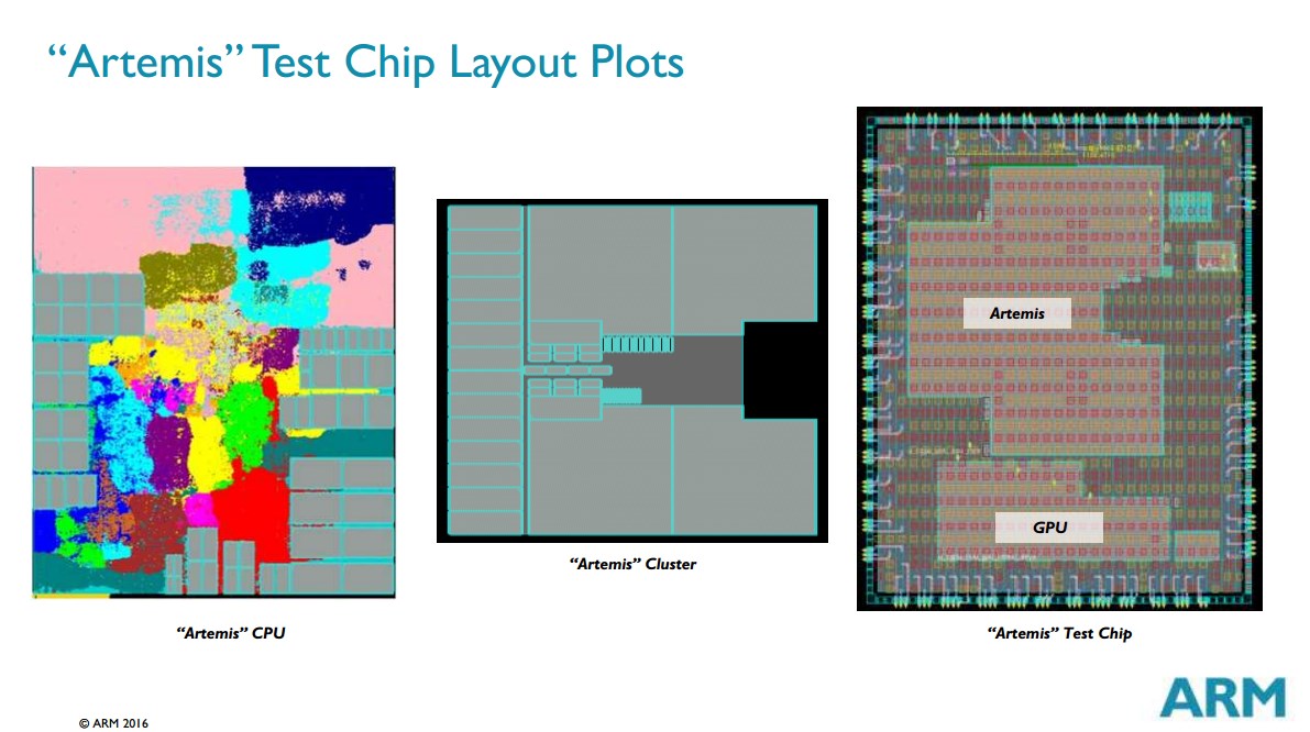
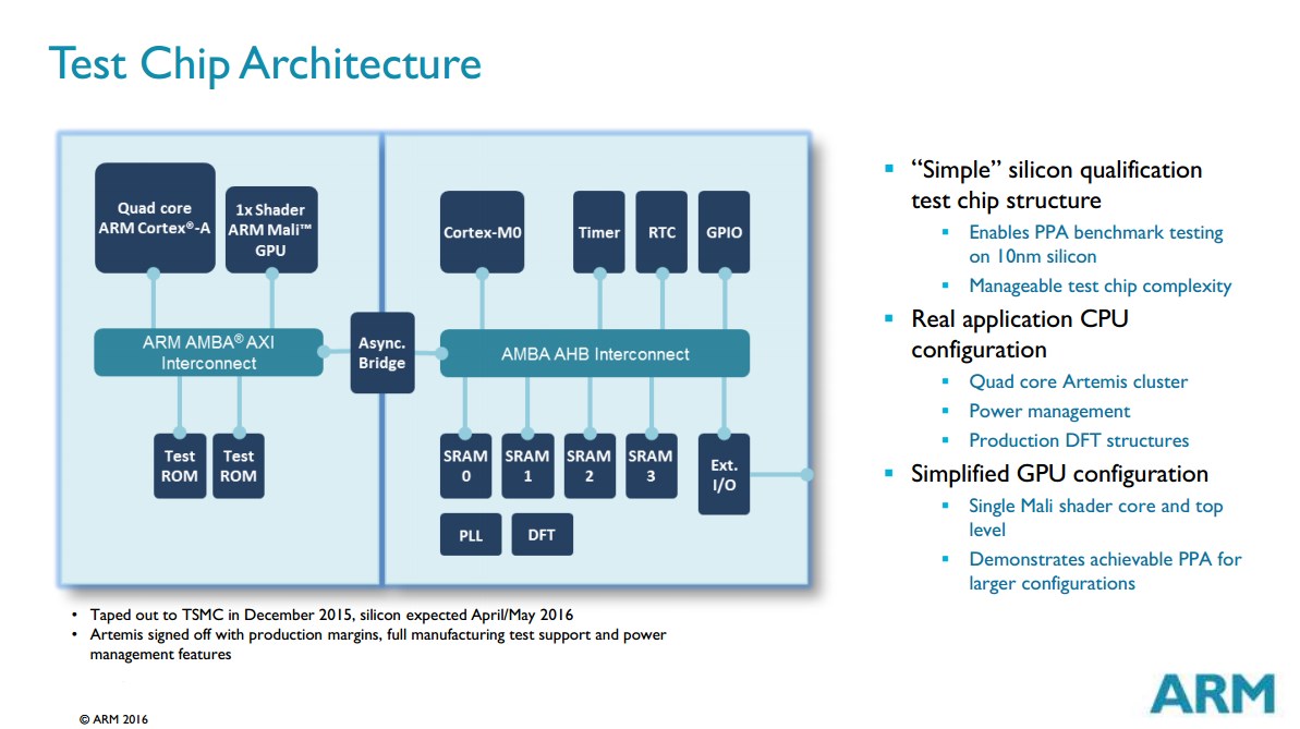
The use of a simple chip design, in this case 4 cores rather than 8, no big.LITTLE, a small GPU etc., is normal for a test chip as the idea here is to test the physical manufacturing processes and not necessarily a full-blown feature rich SoC.

Although we are used to having “silicon chips” in just about everything from a microwave oven to our smartphones, the fabrication of these chips isn’t easy. One of the parameters of fabrication system is known as the “process node” and it defines how small the transistors are and how small the gaps are between transistors. Mid-range SoCs like the Snapdragon 652 or the MediaTek Helio X10 are built using a 28nm (nanometer) process. The Snapdragon 810 used a 20nm process, while Samsung’s Exynos 7420 (from last year’s flag ship devices) and its current Exynos 8890, used a 14nm process, known as 14nm FinFET. To put this into some context, the the process used for the Intel 486 and the lower speed Pentium CPUs was 800nm.
The move to 10nm is a the next step in the drive to shrink the size of the transistors used in the chips. The purpose of the test chip is to ensure that TSMC’s manufacturing processes is full operational and is able to handle the mass production SoCs. It also gives ARM’s partners a head-start when it comes to designing their own SoCs using Artemis, as the lessons learnt from making the test chip will be passed on to them, as well as other important physical design elements like the design flow, methodology, and standard cell libraries.
ARM did the same thing when it launched the Cortex-A72 CPU on 16nm FinFET, a chip that is today used in many flagship devices like the HUAWEI Mate 8 and HUAWEI P9. ARM are also working with TSMC for the next process node after this one, 7nm.
The power/performance ratio of an Artemis CPU built on 10nm will be better than the Cortex-A72 built on 16nm FinFET.
The power/performance ratio of an Artemis CPU built on 10nm will be better than the Cortex-A72 built on 16nm FinFET, which is good for consumers in terms of battery life and the speed of any devices that will use SoC built with Artemis on this process node. The current estimations are that when using 10nm the Artemis CPU can be clocked at around 2.7 or 2.8GHz, however if the same CPU design is built using 16nm (rather than 10nm) the supported clock frequency will actually be higher than the current Cortex-A72 at 16nm.
We will be covering all the full details of the new Artemis core as we learn more, so stay tuned for our coverage of this latest CPU core from ARM.