Affiliate links on Android Authority may earn us a commission. Learn more.
The Age of Graphene and how it will transform our mobile experiences
You may have heard about graphene. Ever since its discovery, scientists have been touting its potential to transform our world. From space elevators to medical nanodevices, the list of potential applications of graphene is huge. But what exactly is graphene? What are its properties and its most interesting applications? And how can it change mobile tech? Let’s dive in!
Graphene: a first of its kind material
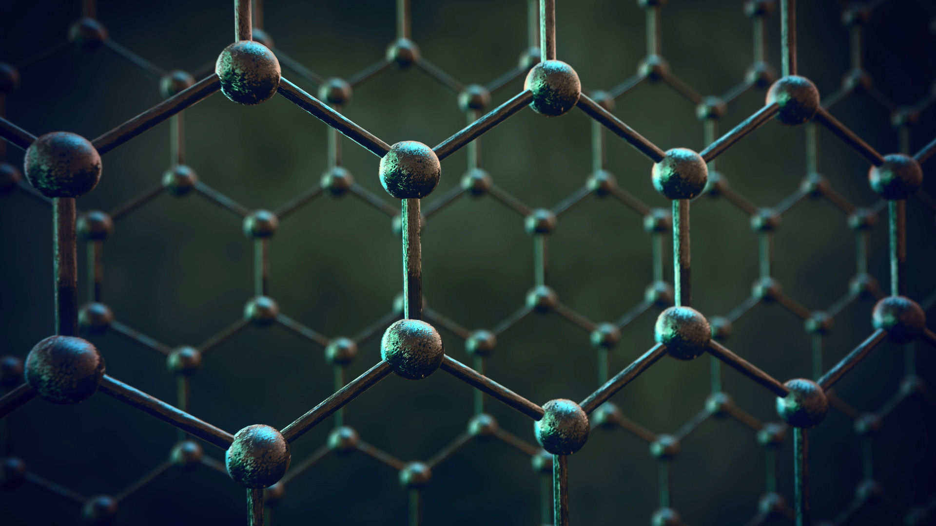
Graphene is the first two-dimensional material known to man. While most materials have a structure featuring atoms arranged in a 3D structure, graphene is made up of a single layer of carbon atoms. In essence, it’s a sheet of carbon with the thickness of one atom.
Graphene was isolated from graphite, which is another form of carbon, in 2004, by two professors from University of Manchester, Andre Geim and Kostya Novoselov. Their work brought them the Nobel Prize in Physics in 2010 (making Novoselov one of the youngest award holders in Physics), when I was still a doctoral student there. This scientific recognition later led to the establishment of UK’s National Graphene Institute, with the goal of pushing graphene research even further.
It’s hard to believe, but the exotic graphene was first obtained through a very basic process, using good old scotch tape! Here’s a visual representation of how it happened.
In essence, one-atom thick graphene crystals were isolated in a Eureka moment by repeatedly applying scotch tape over a strip of charcoal (i.e. carbon), with each application reducing the thickness of the crystals until they were down to an atom thickness. The single layer of atoms forms a 2D honeycomb structure. Fascinatingly, this method works reliably even in home conditions, so go ahead if you want to try yourself – you need some scotch, a graphite pencil lead, and a small microscope to see what you created!
Graphene maintains all the advantages of carbon in terms of being lightweight and strong at the same time ― remember how carbon fiber (combination of carbon cloth with epoxy resin under atmospheric pressure) transformed space and automobile industries thanks to the same properties. Carbon fiber is also making its way into mobile technologies, with companies like Dell and Lenovo using carbon fiber chassis to make laptops that are sturdier and lighter at the same time.
On top of light weight and resistance, graphene has some striking properties which we explore below.
Graphene: Is it the superhero we’ve been waiting for?
The research on various properties and applications of graphene so far suggests that its potential could literally be limitless. In the field of mobile technology, graphene applications range from transparent and flexible screens to next-generation batteries which could last much longer than anything we have experienced so far, to immensely powerful processors.
Graphene-based supercapacitor batteries
Next-generation batteries will move away from electrochemical cells (for example: lithium-ion) towards supercapacitors, which store energy in an electric field instead of a controlled chemical reaction. Supercapacitors achieve much quicker charging times (in the order of seconds) and they are more durable and consistent across a wider temperature range compared to batteries. They are also much more expensive.
Supercapacitors currently take advantage of the high surface area of activated carbon, which helps with the storage and discharging of electrical current. Their performance can be pushed even further by using graphene―also made from pure carbon― which has even higher surface area simply due to its 2D structure.
So far the price range of industrially synthesized graphene is somewhat variable, but the lower price bracket is currently regarded as competitive with the pricing of activated carbon, which means that it can help make supercapacitors more affordable once production volumes increase.
cheap supercapacitors could enable batteries that last for much longer and charge almost instantly
Better battery technology is sorely needed. Thanks to graphene, cheap supercapacitors could enable batteries that last for much longer and charge almost instantly. Such developments would be better for the user experience, but also for the environment. The electricity that we store will be used much more efficiently (and hopefully help us save money on bills). Additionally, battery manufacturing will depend on more ecologically friendly and naturally abundant resources, instead of lithium.
Flexible/foldable screens
Flexible and semitransparent screens are already being introduced by manufacturers such as LG, and rumors suggest Samsung has a foldable smartphone in mind for the future. These novel applications utilize a thin layer of OLEDs incorporated into a flexible sheet of plastic.
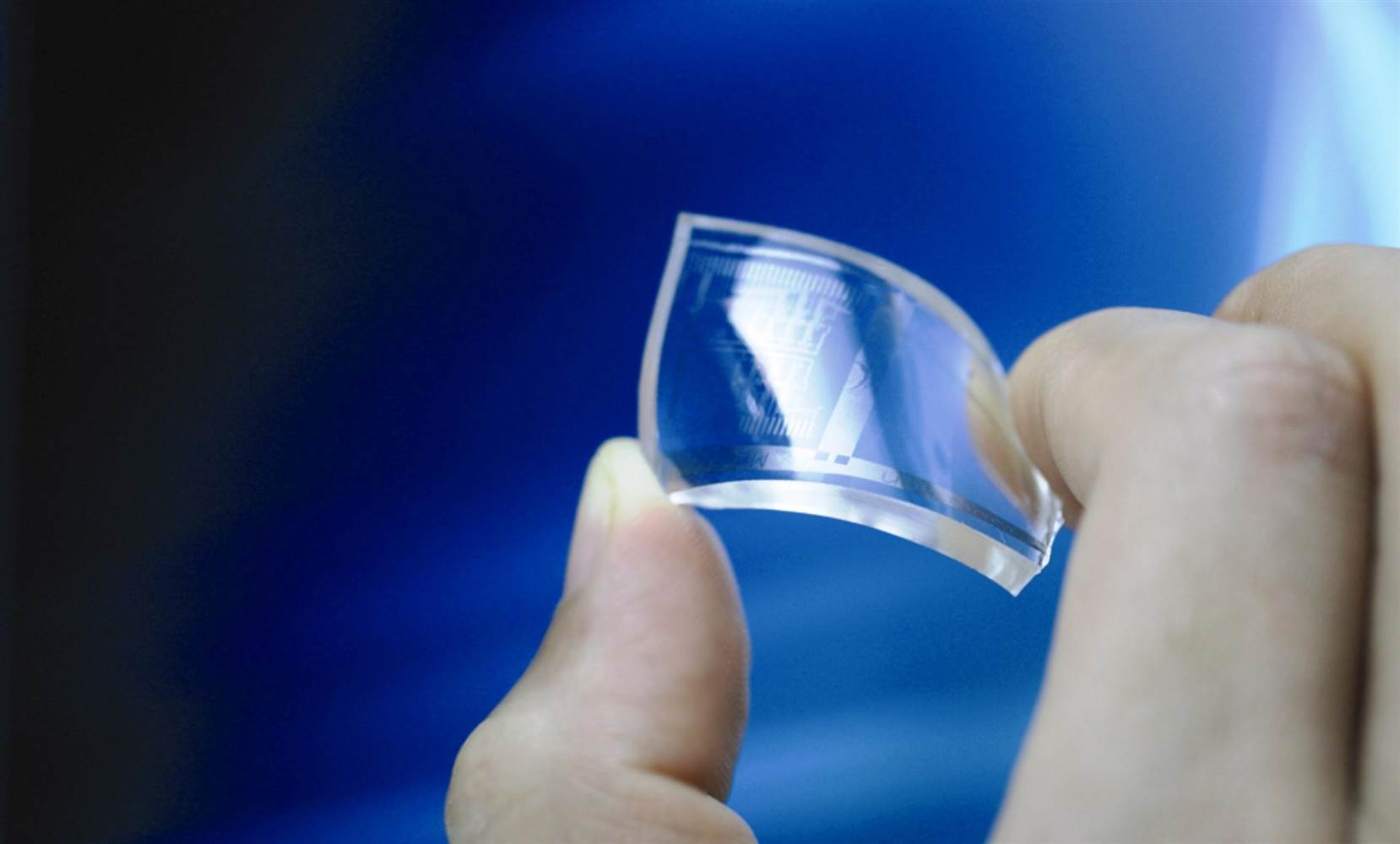
On the material science front, a team led by co-discoverer of graphene Kostya Novoselov designed a 2D LED semiconductor that use LEDs and metallic graphene at an atomic level, resulting in an extremely thin form factor. We have to confess that at the moment it is quite hard to judge how these novel technologies would stack up against each other in real world applications (apart from the fact that graphene based applications would inevitably be thinner).
These novel form factors could be available for consumer use in the next five years. However, we need to wait and see how much demand there will be for flexible and transparent screens in the consumer market.
Shall we say goodbye to the silicon chip?
The research on the electric conducting properties of graphene suggests that its semiconducting properties at room temperature could be manipulated to achieve super-conductance (for example by adding controlled impurities to its natural honeycomb structure). These findings suggest that applications of graphene could particularly be in high demand for various computing technologies, improving speed and efficiency (particularly reducing heating issues). There is more and more research emerging in this field, and the results consistently demonstrate that applications of layers of graphene significantly enhance the thermal performance of microprocessors. In studies, scientists made to reduce operating temperatures by more than 13°C, with every 10°C improvement doubling the energy efficiency. Yes, this means that graphene and other newly discovered 2D materials will eventually transform the silicon chip!
Some of our readers might be thinking, “OK, we all heard rumours about the overheating issues in the first generation of Snapdragon 810, which were later resolved in the second-generation of the SoC, which runs devices such as Nexus 6P and Sony Xperia Z5 series. So what is the big deal about this research and why should we get excited about it?”
The potential of graphene is beyond any significant improvements we observe from one generation of smartphones to the next. Graphene has the potential to transform the landscape of supercomputing in fields such as global climate prediction (consider that global warming is creating more entropy in micro- and macro-climate systems, making predictions more computationally heavy and difficult), space science, big data analysis, and research on artificial intelligence. These are all fields where more computational power and higher efficiency will always be in high demand.

With Internet of Things (IoT) emerging in the last decade, enhancing information processing and connectivity speeds will also transform our daily lives. Hopefully, we will be more likely to stay on top of things in our increasingly hectic and stressful lives. Graphene’s super-conductance property will be one of the key features that will help us achieve higher data processing speeds.
The smartphone as we know it is likely to maintain its form factor and we do not expect massive improvements in speed in every day operation, simply because current processors are already very fast. However, with applications of graphene making their way to market, it’s simple to envision devices like a feather-light version of Google Glass or a smartwatch that’s not 1.2 centimeters in thickness (remember the recently introduced Tag Heuer Connected?) accompanying smartphones. Of course, all device will be efficiently connected and communicating with each other.
Just consider the improvements in Google Now/Siri/Cortana speech recognition in the last two years, and multiply that by a hundred.
In tandem with improvements in cloud supercomputing and connectivity speeds, this trio of devices will be able to host mobile assistants with individually tailored artificial intelligence, that we can interact with in a natural way. Just consider the improvements in Google Now/Siri/Cortana speech recognition in the last two years, and multiply that by a hundred.
Perhaps we should think beyond smartphones, though. I have been recently informed about the development of graphene-based multi electrode arrays (MEA) for surgical implants. These are key components of what is called a brain-machine interface (BMI) in neuroscience. This technology aims to help people with seizures or various diseases of motor control, by sending electric stimulations selectively to certain regions of the brain to compensate for the loss of information due to a neurological disease. These novel MEAs will exploit graphene’s superconductance property, enabling higher transmission speeds and biological compatibility.
This novel direction is fascinating. Consider that Hiroshi Lockheimer, the current head of Android at Google, recently tweeted about a full body ultrasound device which operates on a Samsung Galaxy S6 Edge device. Lockheimer said that Googlers never imagined such possibilities when they launched the first Android phone back in 2008. Similarly, thanks to graphene and other developments, Android devices could one day provide highly personalized assistance to patience in need.

What are the challenges?
This vision of the future that we’ve just painted, and the way mobile technology transformed our lives so far, could bring to mind Huxley’s “Brave New World”. Perhaps this begs a separate discussion. But what about the industrial challenges standing in the way of graphene adoption?
We won’t address all of the challenges we need to overcome, but this excellent article from Nature discusses the opportunities and challenges in detail. That said, production costs, volume manufacturing, and resistance by current technologies are the key challenges that need to be addressed for graphene-based devices to become commonplace.
Could graphene be the super material that we have been waiting for? The short answer is, yes, but it will take time to displace the mature silicon industry. Just like OLED is still not the dominant display technology, even if its superior, graphene based technologies will have to overcome the resistance of the silicon industry. There’s a huge network of companies producing cheap and reliable silicon integrated circuits. An economic battle between established companies and graphene upstarts is brewing.
The greatest advantage of silicone over graphene is 70 years of continuous research behind it
Silicon is a semiconducting element which is quite abundant in nature (making it relatively cheap) and its properties allow easy manipulation of the movement of electrons down the circuit, making it highly suitable for designing electronic chips which should operate reliably in different thermal conditions. So far the greatest advantage of silicone over graphene is 70 years of continuous research behind it, which improved its various industrial applications.
We need more research to discover the true potential of graphene under laboratory conditions before it can reliably be used in various mobile technologies. Although the number of graphene-based patent applications exploded since 2010, it’s still less than a sixth of all silicon related application, which demonstrates why this transition will take time.
On the other hand, considering that graphene consists of carbon, it is much more abundant in nature than silicone and this means that after suitable technology for mass production is established, it would also help towards reducing the costs of making electronic chips.
Ancient inspiration
Some of the readers might be wondering, “OK, we now have a miracle material that we can use in batteries, flexible screens and microprocessors which could transform our lives. You told us that this is in fact a two-dimensional layer, which can be applied on other materials by coating or encapsulating between layers; and it works. But if you want to go further and stack them up one layer after the other, it no longer becomes a two-dimensional layer of graphene, so how can you manufacture 3D objects from a 2D layer?”
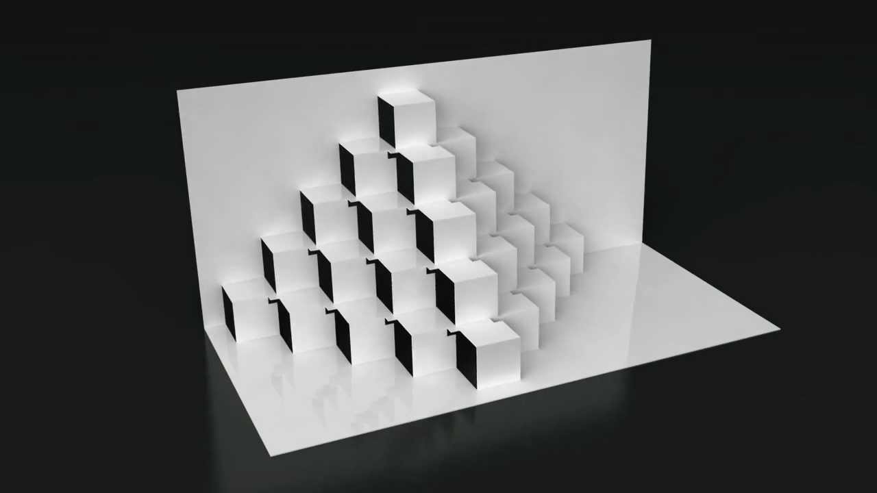
Here, I think it is worthy of mention one recent research which pushed the boundary with outside-the-box thinking. Following laboratory observations suggesting that graphene displays similar properties to paper, physicists at the Cornell University tackled this problem by getting their inspiration from an traditional form Japanese paper cutting art called kirigami. In a recent study published in the acclaimed journal Nature, the researchers used this technique to build 3D structures from the 2D layers of graphene by exploiting its structural strength (which is estimated to be 300 times stronger than steel). Watch the research digest here:
Combining such pyramidal structures with high-end resistors from the tip down the base, it could be fairly straightforward to design gates which will channel high speed information flow within microchips.
Wrap up
The story of graphene started with the good old scotch tape and up-to-date research shows that it is being taken further by traditional paper cutting art. Within the next five years or so, we could witness the end of the Silicon Age and the beginning of the Age of Super-Semiconductors, as advancing research isolates more materials with similar properties to that of graphene, which initiated this transformation. We should all keep our eyes on these advancements which will shape the future of our mobile experience.