Affiliate links on Android Authority may earn us a commission. Learn more.
Road to 4nm: Samsung outlines roadmap to the super fast and efficient chips of tomorrow

Samsung Electronics is already on the cutting edge of foundry process technology and continues to look ahead to the next big breakthrough. The company has just unveiled its plans to bring faster, more power efficient chips to the industry, having outlined its process roadmap down all the way to 4nm.
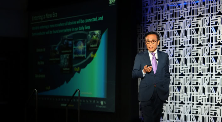
At the Samsung Foundry Forum, the company unveiled its roadmap for a range of major product points, ranging from 28nm technologies down to just 4nm. In order to make these smaller chips a reality, Samsung also confirmed reports that it will be debuting its Extreme Ultraviolet Lithography at these smaller nodes, along with its own Fully Depleted Silicon on SOI (FDSOI) technology for more cost effective 18nm solutions.
In the near future, Samsung plans to roll off revised 14nm and 10nm LPU products, which the company announced in the closing months of 2016, and should enter risk production sometime this year. These revisions are designed to save partners on costs and improve power efficiency. This will be followed up closely by Samsung’s first 8nm LPP technology, which will be the last node based on the company’s current FinFET design. This move will provide both incremental energy and performance benefits over Samsung’s current 10nm process used for today’s high-end smartphone processors.
Samsung to start using EUV
Samsung’s plan to shrink down its chips becomes even more aggressive after 8nm. The company plans to enter risk production of its first 7nm LPP EUV process sometime in 2018, which is faster than many had expected. Foundries have been pushing up against the limits of non-EUV lithography for a while now, so EUV is seen as key to actually realizing performance gains from shrinking processes any further.
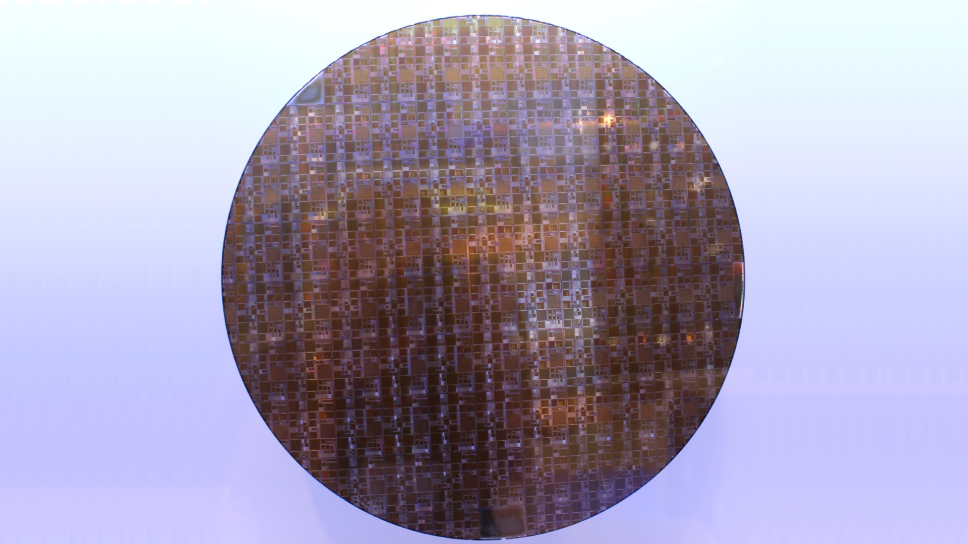
Samsung's upcoming 7nm process will be its first to use Extreme Ultraviolet Lithography technology.
Samsung states that its EUV efforts uses 250W of source power, a key milestone for hitting volume production. The development of which was a collaborative effort between Samsung and ASML. ASML being the company that sells Samsung its photolithography equipment.
Historically, EUV has been held back by high costs and difficulties achieving its high potential etching resolution and yields, so we will have to see if Samsung is able to keep its EUV plans on track. Even so, the company claims that the mask counts and costs will simply be too high to justify any other technology going forward.

A brisk march to 4nm
Once EUV makes its debut at 7nm, Samsung plans to quickly follow up with smaller and smaller process nodes, targeting 6nm, 5nm, and 4nm respectively. 6nm and 5nm are expected to tail just a year behind the company’s 7nm plans. Samsung says that 6nm LPP will incorporate its Smart Scaling solutions for better area efficiency, while 5nm LPP will be the company’s smallest FinFET solution that will also incorporating some innovations from its 4nm technology for better power savings.
Based on Samsung’s targets, its 4nm LPP technology could enter risk production as early as 2020. As well as shrinking transistors down further, the move to 4nm also comes with a switch to a next generation device architecture dubbed Multi Bridge Channel FET (MBCFET). MBCFET is Samsung’s unique Gate All Around FET technology designed as a successor to the current FinFET architecture. MBCFET makes use of a Nanosheet device to overcome the physical scaling and performance limitations of FinFET, allowing Samsung to hit 4nm in conjunction with EUV.

Talking of timeframes, I should note that there’s no specific time link between risk production targets, volume production, and products hitting the shelves, and it varies from foundry to foundry. Usually volume can be ramped up in the months following final yield tests, but then there’s always a further delay between chips rolling off the line and customers buying products. So at best, peg these products for a consumer release a year later than the dates listed here, barring any delays.
Lower costs and IoT
The final announcement from the Samsung Foundry Forum is news of new Fully Depleted Silicon on Insulator (FDSOI) processes. These products are intended for consumers looking for more budget oriented chips or those that don’t require cutting edge nodes. This move could make Samsung a more competitive choice to the likes of GlobalFoundries too.
Samsung is planning to extend its current 28nm option first by incorporating radio frequency and then eMRAM options, which it believes will be well suited for Internet-of-Things applications. This is to be followed up by a smaller 18nm process, which will offer enhanced performance, power, and area efficiency over the 28nm generations. Again, this process will be augmented up with RF and eMRAM options a year later, which could appear around the same time as Samsung’s 4nm.

The final word
Clearly, Samsung is undertaking an aggressive strategy in the race to smaller process nodes, aiming to be first to both 7nm and then 4nm. Not that we should be too surprised, given the huge investments that the company has been making into its chip production facilities lately. The introduction of EUV is important going forward, but how well refined this technology has become will be the crucial factor in determining if Samsung is able to stick to its ambitious roadmap.
In the mobile space, Samsung has been on top since the quick introduction of its 14nm FinFET technology and clearly wants to remain in pole position. We will have to see how TSMC, Intel, Qualcomm, and others react to Samsung’s plans.