Affiliate links on Android Authority may earn us a commission. Learn more.
Display technology explained: A-Si, LTPS, amorphous IGZO, and beyond
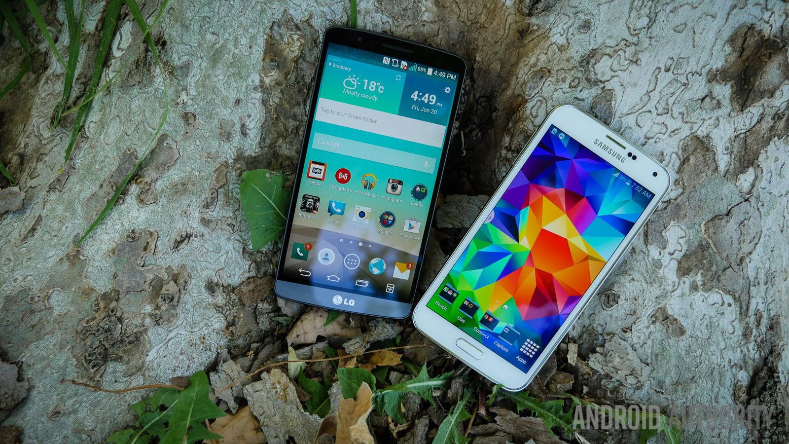
LCD or AMOLED, 1080p vs 2K? There are plenty of contentious topics when it comes to smartphone displays, which all have an impact on the day to day usage of our smartphones. However, one important topic which is often overlooked during analysis and discussion is the type of backplane technology used in the display.
Display makers often throw around terms like A-Si, IGZO, or LTPS. But what do these acronyms actually mean and what’s the impact of backplane technology on user experience? What about future developments?
For clarification, backplane technology describes the materials and assembly designs used for the thin film transistors which drive the main display. In other words, it is the backplane that contains an array of transistors which are responsible for turning the individual pixels on and off, acting therefore as a determining factor when it comes to display resolution, refresh rate, and power consumption.
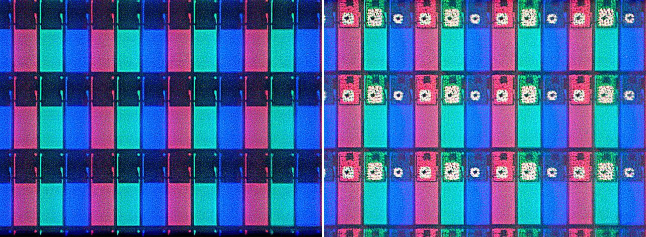
Examples of backplane technology include amorphous silicon (aSi), low-temperature polycrystalline silicon (LTPS) and indium gallium zinc oxide (IGZO), whilst LCD and OLED are examples of light emitting material types. Some of the different backplane technologies can be used with different display types, so IGZO can be used with either LCD or OLED displays, albeit that some backplanes are more suitable than others.
a-Si
Amorphous silicon has been the go-to material for backplane technology for many years, and comes in a variety of different manufacturing methods, to improve its energy efficiency, refresh speeds, and the display’s viewing angle. Today, a-Si displays make up somewhere between 20 and 25 percent of the smartphone display market.
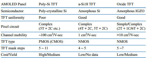
For mobile phone displays with a pixel density lower than 300 pixels per inch, this technology remains the preferable backplane of choice, mainly due to its low costs and relatively simple manufacturing process. However, when it comes to higher resolution displays and new technologies such as AMOLED, a-Si is beginning to struggle.
AMOLED puts more electrical stress on the transistors compared with LCD, and therefore favours technologies that can offer more current to each pixel. Also, AMOLED pixel transistors take up more space compared with LCDs, blocking more light emissions for AMOLED displays, making a-Si rather unsuitable. As a result, new technologies and manufacturing processes have been developed to meet the increasing demands made of display panels over recent years.
LTPS
LTPS currently sits as the high-bar of backplane manufacturing, and can be spotted behind most of the high end LCD and AMOLED displays found in today’s smartphones. It is based on a similar technology to a-Si, but a higher process temperature is used to manufacture LTPS, resulting in a material with improved electrical properties.
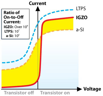
LTPS is in fact the only technology that really works for AMOLED right now, due to the higher amount of current required by this type of display technology. LTPS also has higher electron mobility, which, as the name suggests, is an indication of how quickly/easily an electron can move through the transistor, with up to 100 times greater mobility than a-Si.
For starters, this allows for much faster switching display panels. The other big benefit of this high mobility is that the transistor size can be shrunk down, whilst still providing the necessary power for most displays. This reduced size can either be put towards energy efficiencies and reduced power consumption, or can be used to squeeze more transistors in side by side, allow for much greater resolution displays. Both of these aspects are becoming increasingly important as smartphones begin to move beyond 1080p, meaning that LTPS is likely to remain a key technology for the foreseeable future.

The drawback of LTPS TFT comes from its increasingly complicated manufacturing process and material costs, which makes the technology more expensive to produce, especially as resolutions continue to increase. As an example, a 1080p LCD based on this technology panel costs roughly 14 percent more than a-Si TFT LCD. However, LTPS’s enhanced qualities still mean that it remains the preferred technology for higher resolution displays.
IGZO
Currently, a-Si and LTPS LCD displays make up the largest combined percentage of the smartphone display market. However, IGZO is anticipated as the next technology of choice for mobile displays. Sharp originally began production of its IGZO-TFT LCD panels back in 2012, and has been employing its design in smartphones, tablets and TVs since then. The company has also recent shown off examples of non-rectangular shaped displays based on IGZO. Sharp isn’t the only player in this field — LG and Samsung are both interested in the technology as well.
The area where IGZO, and other technologies, have often struggled is when it comes to implementations with OLED. ASi has proven rather unsuitable to drive OLED displays, with LTPS providing good performance, but at increasing expense as display size and pixel densities increase. The OLED industry is on the hunt for a technology which combines the low cost and scalability of a-Si with the high performance and stability of LTPS, which is where IGZO comes in.
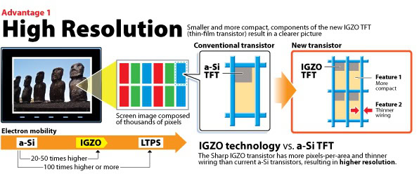
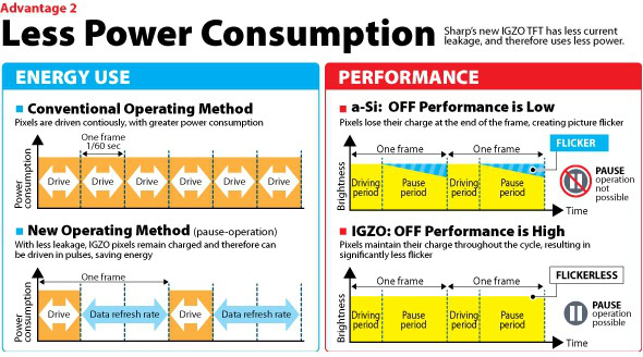
Why should the industry make the switch over to IGZO? Well, the technology has quite a lot of potential, especially for mobile devices. IGZO’s build materials allow for a decent level of electron mobility, offering 20 to 50 times the electron mobility of amorphous silicon (a-Si), although this isn’t quite as high as LTPS, which leaves you with quite a few design possibilities. IGZO displays can therefore by shrunk down to smaller transistor sizes, resulting in lower power consumption, which provides the added benefit of making the IGZO layer less visible than other types. That means you can run the display at a lower brightness to achieve the same output, reducing power consumption in the process.
One of IGZO’s other benefits is that it is highly scalable, allowing for much higher resolution displays with greatly increased pixel densities. Sharp has already announced plans for panels with 600 pixels per inch. This can be accomplished more easily than with a-Si TFT types due to the smaller transistor size.
Higher electron mobility also lends itself to improved performance when it comes to refresh rate and switching pixels on and off. Sharp has developed a method of pausing pixels, allowing them to maintain their charge for longer periods of time, which again will improve battery life, as well as help create a constantly high quality image.
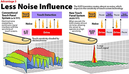
Smaller IGZO transistors are also touting superior noise isolation compared to a-Si, which should result in a smoother and more sensitive user experience when used with touchscreens. When it comes to IGZO OLED, the technology is well on the way, as Sharp has just unveiled its new 13.3-inch 8K OLED display at SID-2014.
Essentially, IGZO strives to reach the performance benefits of LTPS, whilst keeping fabrications costs as low as possible. LG and Sharp are both working on improving their manufacturing yields this year, with LG aiming for 70% with its new Gen 8 M2 fab. Combined with energy efficient display technologies like OLED, IGZO should be able to offer an excellent balance of cost, energy efficiency, and display quality for mobile devices.
What’s next?
Innovations in display backplanes aren’t stopping with IGZO, as companies are already investing in the next wave, aiming to further improve energy efficiency and display performance. Two examples worth keeping an eye are on are Amorphyx’ amorphous metal nonlinear resistor (AMNR) and CBRITE.

Starting with AMNR, a spin-off project which came out of Oregon State University, this technology aims to replace the common thin-film transistors with a simplified two-terminal current tunnelling device, which essentially acts as a “dimmer switch”.
This developing technology can be manufacturing on a process that leverages a-Si TFT production equipment, which should keep costs down when it comes to switching production, whilst also offering a 40 percent lower cost of production compared with a-Si. AMNR is also touting better optical performance than a-Si and a complete lack of sensitivity to light, unlike IGZO. AMNR could end up offering a new cost effective option for mobile displays, while making improvements in power consumption too.
CBRITE, on the other hand, is working on its own metal oxide TFT, which has a material and process that delivers greater carrier mobility than IGZO. Electron mobility can happily reach 30cm²/V·sec, around the speed of IGZO, and has been demonstrated reaching 80cm²/V·sec, which is almost as high as LTPS. CBRITE also appears to lend itself nicely to the higher resolution and lower power consumption requirements of future mobile display technologies.

Furthermore, this technology is manufactured from a five-mask process, which reduces costs even compared to a-Si and will certainly make it much cheaper to manufacture than the 9 to 12 mask LTSP process. CBITE is expected to start shipping products sometime in 2015 or 2016, although whether this will end up in mobile devices so soon is currently unknown.
Smartphones are already benefiting from improvements in screen technology, and some would argue that things are already as good as they need to be, but the display industry still has plenty to show us over the next few years.