Affiliate links on Android Authority may earn us a commission. Learn more.
Samsung realizes big power savings with its 14nm Exynos 7420 SoC
Published onJune 29, 2015

Samsung’s Galaxy S6 flagship has been topping the performance benchmarks since its release, thanks to the company’s in house Exynos 7420 system-on-a-chip. The chip is built on the industry’s smallest 14nm manufacturing process, allowing for greater processing performance in a more energy efficient package.
The clever folks over at AnandTech have put together a comprehensive deep-dive into the inner workings of Samsung’s cutting edge 14nm processor. Be sure to check out the full article for a major geeky breakdown of the ins-and-outs, we are going to take a closer look at perhaps the most important aspect for us consumers – the power savings.
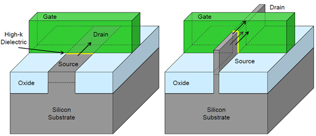
For a quick recap, Samsung built the Exynos 7420 SoC on its latest 14nm FinFET fabrication process, besting TSMC’s 28nm and 20nm processes used for Qualcomm and MediaTek chips. Essentially, smaller manufacturing process helps to reduce silicon area, and improve performance and energy efficiency due to the smaller distances between components.

In terms of space savings against the similarly specced Samsung Exynos 5433, Samsung’s 14nm process has seen a huge area reduction of 70 percent for the clusters of Cortex-A57 and A53 CPU cores. The GPU cluster saw its size shrink by an impressive 41 percent also, but remember that the 14nm Exynos 7420 uses eight shader cores in its designed, compared with six for the 20nm Exynos 5433.
On a per core basis, Samsung looks to have made a similar 76 percent size reduction in the GPU department. The total die size for the Exynos 7420 comes in at just 78mm2, compared with 133mm2 for the last generation Exynos 5433, a total shrink of around 44 percent.
Samsung had produced a healthy power saving in both big.LITTLE clusters, approaching 50 percent when the A57 is clocked at higher frequencies
Samsung has been able to make major savings on area and this translates into a direct power saving in the CPU and GPU core clusters. Overall, the Exynos 7420 caps out at around 1W when fully loading up 4 threads in the Cortex-A53 cluster. Maximum power consumption of the A57 cores comes in at a much higher 5.49W, but this is improved over the Exynos 5433’s 7.39W peak draw. We certainly don’t expect all four A57 cores to be running at such high speeds for very long, and our real world Global Task Scheduling (GTS) tests showed this to be the case.
The improvements can be best seen by directly comparing the average per core power consumption of the Exynos 5433 with the 7420, minus any non-CPU consumption such as cluster, interconnect and memory overheads.

Also, note the drastic difference in power consumption between the A57 and A53 cores for the same clock frequency. We’re looking at around a quarter of power consumption of a 1 GHz A57 with a similarly clocked A53, which is an important point to appreciate with the big.LITTLE architecture.
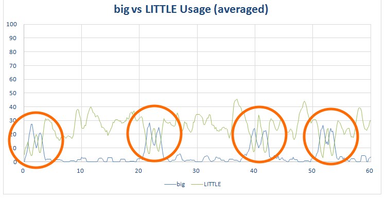
There’s more to CPU efficiency than just raw power consumption though, Samsung has been working on improving GTS with its latest Exynos chip. As we have already seen from our look at the Galaxy S6’s big.LITTLE workloads, the handset’s power management system appears better than previous generation Exynos processors. By power mangagement and GTS we mean dynamic allocation of loads between the low power A53 and high performance A57 CPU cores.
Looking at the way the Exynos 5433 and 7420 are setup, it’s clear that Samsung now has a much better handle on how to eke out better efficiency from its new design. Ideally, the cores should switch over at near identical performance per Watt points. This would allow for a full ramp up through performance levels with a mostly consistent increase in power consumption.

Testing found a notable gap with the 5433 implementation, which results in a big jump in performance and power consumption between the big and LITTLE clusters. Samsung has managed to get much closer to the ideal implementation with the 7420 and the move to 14nm has certainly helped with this.
Things are quite a bit simpler on the GPU side, with the power saving from the move to 14nm being put towards an additional 2 shader cores. Heavy GPU loads push power consumption up to around 4.9W in Samsung’s latest chip, which is lower than the higher peak power draw of 5.8W for the Snapdragon 810’s Adreno 430 GPU and 6.1W for the Exynos 5433’s Mali-T760 MP6 configuration.
Heavy GPU loads push power consumption up to around 4.9W in Samsung's latest chip.
However, AnandTech noted that throttling eventually takes place to keep the chip in a more reasonable 3-4W range, which limits the GPU to 350-420MHz states, rather than its peak at 772MHz. This isn’t a phenomenon limited to Samsung’s design, most SoC designers are pushing the limits of GPU TDP for mobile, possibly to ensure healthy looking scores in short term benchmark tests.
All of the above said, there’s a lot more going on in a handset than just the SoC and the display still remains one of the largest power hungry components. The Galaxy S6 draws 358mW with minimal draw from the display, which is less than the Note 4’s 452mW and the HUAWEI P8’s 500mW. However, it falls behind the 258mW power consumption of the Galaxy S5, most likely because of the increased power demands of a QHD display.
Samsung’s latest SoC is clearly a major step forwards for power efficiency. But in the end, the company opted to push for more performance and energy hungry display components, rather than setting these saving aside for a major boost in battery life. The Exynos 7420 is going to be the target to beat when Qualcomm rolls out its next generation mobile SoCs built on an equivalent manufacturing process.