Affiliate links on Android Authority may earn us a commission. Learn more.
How Google is powering the world's AI
Published onNovember 25, 2017
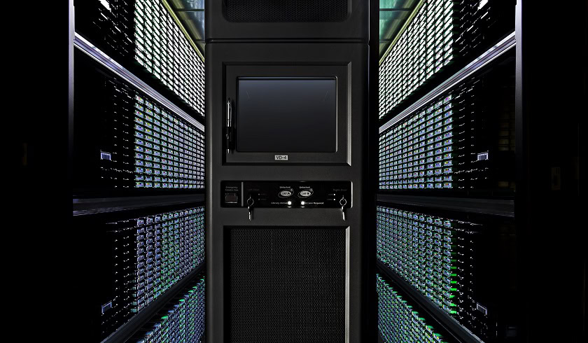
Neural networking algorithms and machine learning are already at the heart of many of Google’s services. They filter out spam in Gmail, optimize targeted advertising, and analyze your voice when you talk to Google Assistant or your Home speaker. Inside smartphones, ideas like Google Lens and Samsung’s Bixby are showing the power of “AI” vision processing. Even companies like Spotify and Netflix are using Google’s Cloud servers to tailor content to their users.
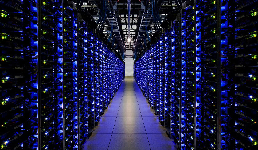
Google’s Cloud Platform is at the center of its efforts (and those of third parties) to utilize this increasingly popular area of computing. However, this new field requires new kinds of hardware to run efficiently, and Google has invested heavily in its own processing hardware, which it calls a cloud tensor processing unit (Cloud TPU). This custom hardware is packed into Google’s servers and already powers the current and expanding AI ecosystem. But how does it work?
TPUs vs CPUs – searching for better efficiency
Google unveiled its second-generation TPU at Google I/O earlier this year, offering increased performance and better scaling for larger clusters. The TPU is an application specific integrated circuit. It’s custom silicon designed very specifically for a particular use case, rather than a general processing unit like a CPU. The unit is designed to handle common machine learning and neural networking calculations for training and inference; specifically matrix multiply, dot product, and quantization transforms, which are usually just 8 bits in accuracy.
While these kinds of calculations can be done on a CPU and sometimes even more efficiently on a GPU, these architectures are limited in terms of performance and energy efficiency when scaling across operation types. For example, IEEE 754 8-bit integer multiplication optimized designs can be up to 5.5X more energy and 6X more area efficient than 16-bit floating-point optimized designs. They’re also 18.5X more efficient in terms of energy and 27X smaller in terms of area than 32-bit FP multiply. IEEE 754 being the technical standard for floating point computations used in all modern CPUs.
Furthermore, many neural networking use cases require low latency and almost instantaneous processing times from a user perspective. This favors dedicated hardware for certain tasks, as opposed to trying to fit typically higher latency graphics architectures to new use cases. Memory latency accessing external RAM can be hugely costly too.
In large data centers, power and silicon hungry processors quickly rack up costs. Google's TPU is designed in equal parts for efficiency as well as performance.
In large data centers, the power and area inefficiencies when performing neural networking functions on a CPU or GPU could result in huge costs. Not just in terms of silicon and equipment, but also the energy bill over long periods of time. Google knew that if machine learning was ever to take off in a meaningful way, it needed hardware that could offer not only high performance, but also substantially better energy efficiency than leading CPUs and GPUs could offer.
To solve this problem, Google set about designing its TPU to offer a tenfold cost-performance improvement over an off-the-shelf GPU. The final design was a co-processor that could be attached to the common PCIe bus, allowing it to work alongside a regular CPU, which would pass it instructions and handle traffic, among other things, as well as help speed up deployment times by making the design an add-on. As a result, the design was up and running in data centers just 15 months after conception.
TPU deep dive
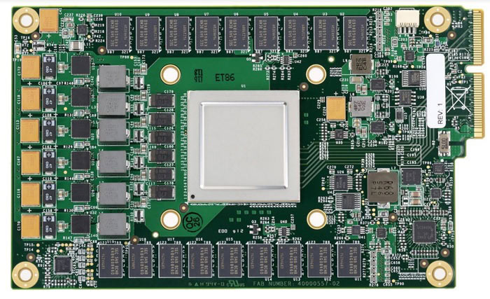
Earlier in the year, Google released a comprehensive comparison of its TPU’s performance and efficiencies compared with Haswell CPUs and NVIDIA Tesla K80 GPUs, giving us a closer look at the processor’s design.

At the heart of Google’s TPU is a Matrix Multiply Unit. The unit contains 65,538 8-bit multiplier accumulators (MACs)— hardware units designed specifically to calculate the product of two numbers and add that to an accumulator. When done with floating point numbers, this is called a fused multiply-add (FMA). You may recall that this is an instruction that ARM has made efforts to optimize with its latest Cortex-A75 and A55 CPUs, as well as Mali-G72 GPU.
Unlike a CPU or GPU, which accesses multiple registers per operation when sending data to and from their arithmetic logic units (ALUs), this MAC implements a systolic design that reads a register once and reuses that value throughout a prolonged calculation. This is possible in the TPU because of its simplified design that sees the ALUs perform multiplication and addition in fixed patterns across adjoining ALUs, without needing any memory access. This limits the design in terms of possible functions, but greatly increases its performance and power efficiency at these fused-multiply tasks.
In terms of numbers, Google’s TPU can process 65,536 multiply-and-adds for 8-bit integers every cycle. Given that the TPU runs at 700MHz, it can compute 65,536 × 700,000,000 = 46 × 1012 multiply-and-add operations or 92 TeraOps (trillions of operations) per second in the matrix unit. Google says that its second generation TPU can deliver up to 180 teraflops of floating point performance. That’s significantly more parallel throughput than your typical scalar RISC processor, which usually only passes a single operation with each instruction over a clock cycle or more.
The 16-bit products of the Matrix Multiply Unit are collected in the 4 MiB of 32-bit Accumulators below the matrix unit. There’s also a unified buffer of 24MB of SRAM, which work as registers. Instructions to control the processor are sent from a CPU to the TPU via the PCIe bus. These are complex CISC type instructions in order to run complex tasks which each instruction, such as numerous multiply-add calculations. These instructions are passed down a 4-stage pipeline. There are only twelve instructions for the TPU in total, the five most important of which are simply to read and write results and weights in memory, and to begin a matrix multiply/convolution of the data and weights.
At the heart of Google’s TPU is a Matrix Multiple Unit, capable of 92 trillion operations per second, but otherwise the microarchitecture is a surprisingly streamlined design. It's built to only handle a small number of operations, but can perform them very quickly and efficiently.
Overall, Google’s TPU much more closely resembles the old idea of a floating-point co-processor than a GPU. It’s a surprisingly streamlined piece of hardware, consisting of only one major processing element and a small simplified control scheme. There are no caches, branch predictors, multi-processing interconnects, or other microarchitectural features that you’ll find in a common CPU. This again helps to save significantly on silicon area and power consumption.
In terms of performance, Google states that its TPU design typically delivers an 83x better performance-to-watt ratio compared with a CPU, and 29x better than when running on a GPU. Not only is the chip design more energy efficient, but it delivers better performance too. Across six common reference neural networking workloads, the TPU offers substantial performance benefits in all but one of the tests, often by a magnitude of 20x or faster compared to a GPU and up to 71x faster than a CPU. Of course, these results will vary depending on the type of CPU and GPU tested, but Google conducted its own tests against the high-end Intel Haswell E5-2699 v3 and NVIDIA K80 for its in-depth look at the hardware.
Working with Intel for edge compute
Google’s hardware efforts have given it a major head start in the cloud space, but not all AI applications are well suited to transferring data such great distances. Some applications, such as self driving cars, require almost instantaneous compute, and so can’t rely on higher latency data transfers over the internet, even if the compute power in the cloud is very fast. Instead, these type of applications need to be done on device, and the same applies for a number of smartphone applications, such as image processing on RAW camera data for a picture.
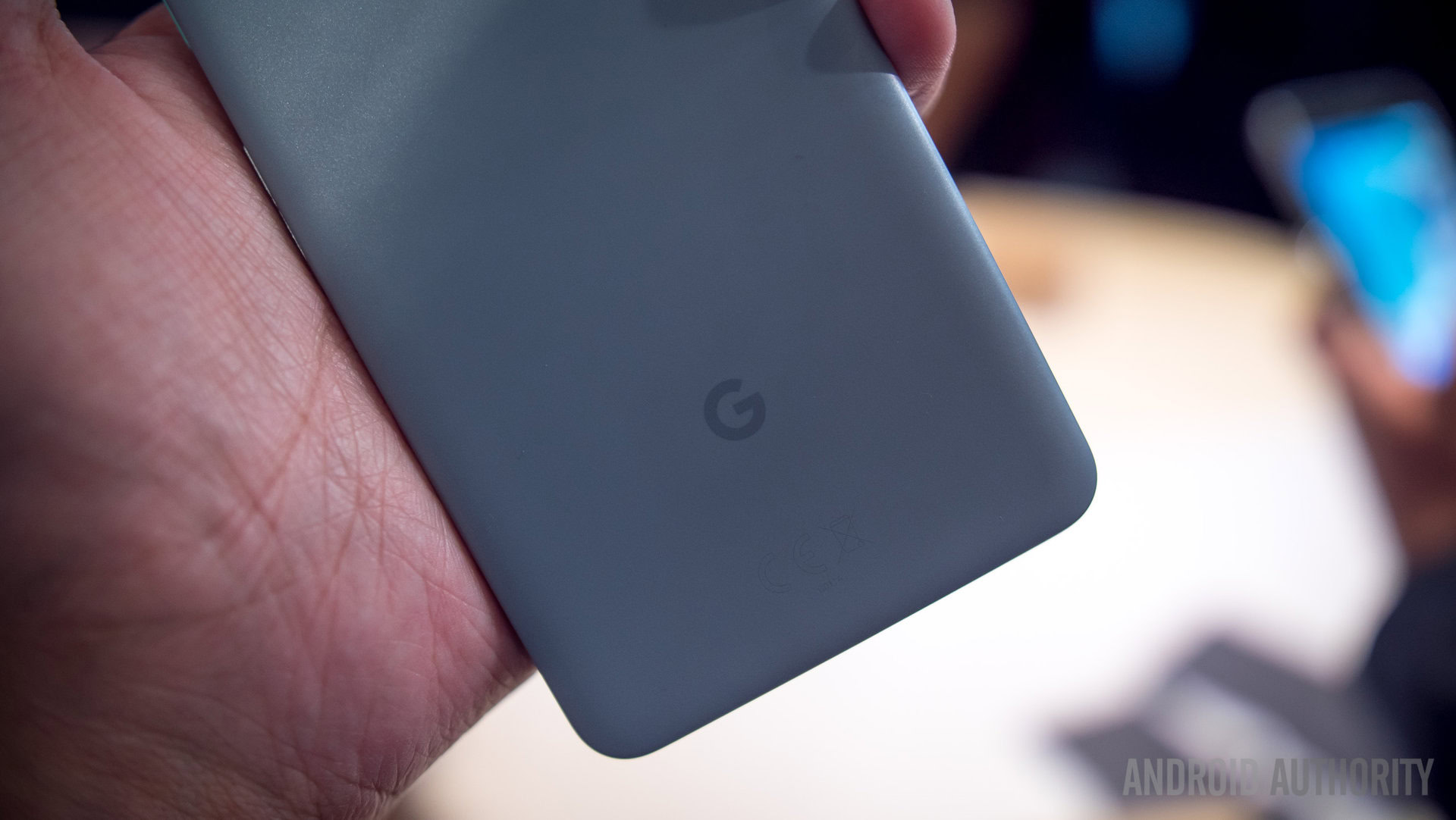
Google's Pixel Visual Core is primarily designed for HDR image enhancement, but the company has touted its potential for other future machine learning and neural networking applications.
With the Pixel 2, Google quietly launched its first attempt at bringing neural networking capabilities to dedicated hardware suitable for a lower power mobile form factor – the Pixel Visual Core. Interestingly, Google teamed up with Intel for the chip, suggesting that it wasn’t entirely an in-house design. We don’t know exactly what the partnership entails; it could just be architectural or more to do with manufacturing connections.
Intel has been buying up AI hardware companies, nabbing Nervana Systems in 2016, Movidius (which made chips for DJI drones) last September, and Mobileye in March 2017. We also know that Intel has its own neural networking processor in the works, codenamed Lake Crest, which falls under its Nervana line. This product was the result of Intel’s purchase of the company of the same name. We don’t know a lot about processor, but it’s designed for servers, uses a low-precision number format called Flexpoint, and boasts a blazing fast memory access speed of 8 Terabits per second. It’s going to compete with Google’s TPU, rather than it’s mobile products.
Even so, there appear to be some design similarities between Intel and Google hardware based on images floating around online. Specifically, the multi-core configuration, use of PCIe and accompanying controller, a management CPU, and close integration to fast memory.
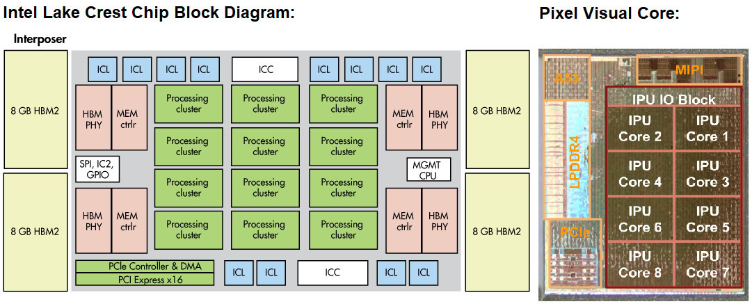
At a glance, the Pixel’s hardware looks quite different to Google’s cloud design, which isn’t surprising given the different power budgets. Although we don’t know as much about the Visual Core architecture as we do about Google’s Cloud TPUs, we can spot some similar capabilities. Each of the Image Processing Units (IPUs) inside the design offers 512 arithmetic logic units, for a total of 4,096.
Again, this means a highly parallelized design capable of crunching lots of numbers at once, and even this trimmed down design can perform 3 trillion operations per second. Clearly the chip features a far smaller number of math units than Google’s TPU, and there are no doubt other differences as this is primarily designed for imaging enhancements, rather than the variety of neural networks Google is running in the cloud. However, it’s a similar, highly parallel design with a specific set of operations in mind.
Whether Google sticks with this design and continues to work with Intel for future edge compute capabilities, or returns to relying on hardware developed by other companies remains to be seen. However, I would be surprised if we don’t see Google’s experience in neural networking hardware continue to evolve silicon products both in the server and small form factor spaces.

Wrap Up
The company’s custom TPU silicon provides the necessary energy efficiency savings needed to deploy machine learning on a large cloud scale. It also offers up notably higher performance for these specific tasks than more generalized CPU and GPU hardware. We’re seeing a similar trend in the mobile space, with SoC manufacturing increasingly turning to dedicated DSP hardware to efficiently run these mathematically intensive algorithms. Google could become a major hardware player in this market too.
We’re still waiting to see what Google has in store for its first generation smartphone AI hardware, the Pixel Visual Core. The chip will soon be switched on for faster HDR processing and will no doubt play a role in some further AI tests and products that the company rolls out to its Pixel 2 smartphones. At the moment, Google is leading the way forward with its Cloud TPU AI hardware and software support with TensorFlow. It’s worth remembering that Intel, Microsoft, Facebook, Amazon, and others are all vying for a piece of this quickly emerging market too.
With machine learning and neural networks powering an increasing number of applications both in the cloud and on edge devices like smartphones, Google’s early hardware efforts have positioned the company to be a leader in this next generation field of computing.