Affiliate links on Android Authority may earn us a commission. Learn more.
IBM announces the world's first working 7nm chip
Published onJuly 10, 2015

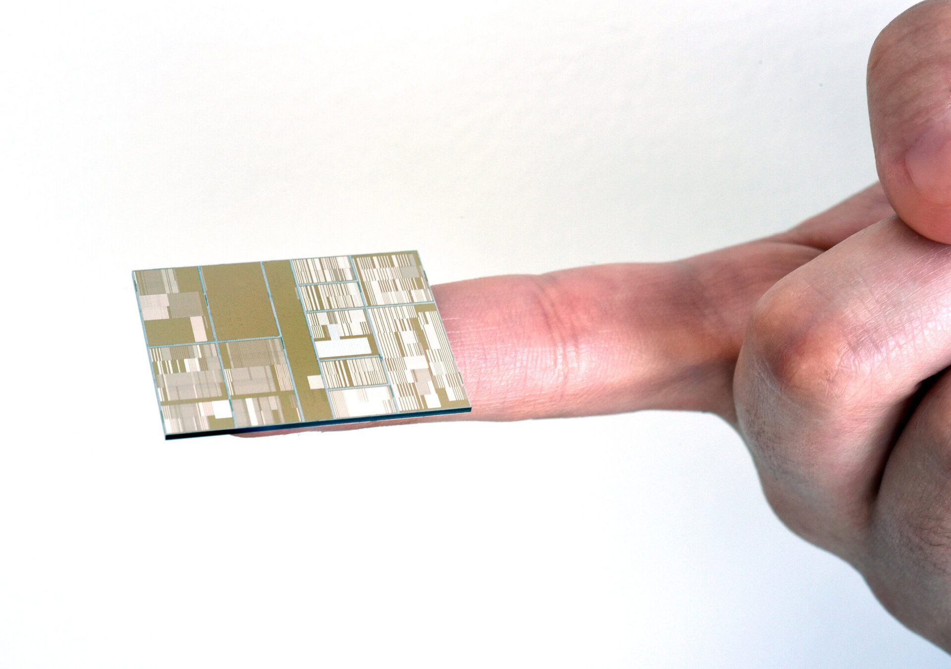
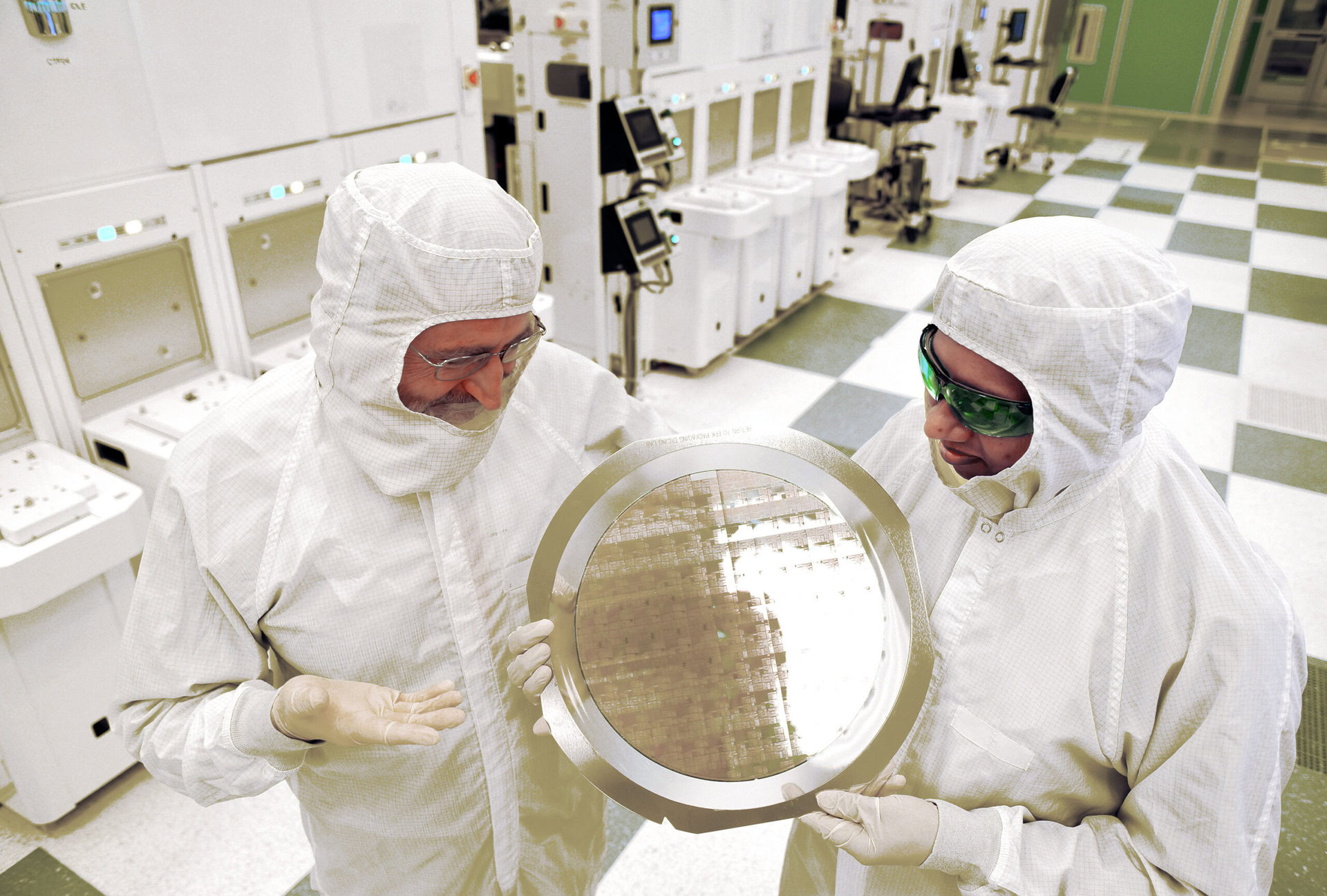
IBM, in conjunction with GlobalFoundries, Samsung and SUNY, has unveiled the world’s first successful production of a 7nm FinFET chip with fully working transistors. The achievement comes as part of a $3 billion, five year research program spearheaded by IBM, which aims to push the limits of chip technology.
Today’s leading mobile processors are built on 14nm and 20nm manufacturing techniques. This 7nm breakthrough will eventually lead to smaller, faster and more energy efficient processors. However, before we go any further, it’s important to note that we are still years away from any potentially viable mass manufacturing techniques at 7nm.
Just yesterday we were talking about the ongoing race to 10nm, but to reach even smaller chip sizes we’re going to need new manufacturing techniques and new materials, plain old silicon just won’t cut it here. This is where IBM’s research comes in.
For a little background, one of the difficulties associated with smaller transistors (the electronic switches that form that basis of processors) is that the number of electrons able to squeeze through the transistor (aka the current) is also reduced, which increases the chance of errors. To combat this issue, IBM mixed some germanium into the channel, producing a silicon-germanium (SiGe) alloy with higher electron mobility, thereby improving the current flow. SiGe also helps to keep power consumption low and transistor switching at high speeds.

The other half of successfully producing such small chips is actually developing manufacturing tools detailed and accurate enough to etch out your processor design on such a small scale. IBM made its chip using EUV lithography, which uses a wavelength of just 13.5nm to etch out chip features. This is substantially smaller than the 193nm wavelength of state of the art argon fluoride lasers used at 14nm.
However, EUV is still expensive and difficult to use, making its suitability for time constrained mass production questionable. The tiniest errors at this size can completely undermine production, so expensive stabilizing isolation equipment and buildings are required to protect the manufacturing tools from vibrations. Some observers are concerned about the diminishing savings associated with ever smaller processors, as difficult and more expensive manufacturing techniques eat into the cost benefits of being able to squeeze more chips onto the same silicon area.
It is still too early to say when 7nm mass production capabilities will be ready, but firms have their sights set for sometime around 2017/2018.