Affiliate links on Android Authority may earn us a commission. Learn more.
MicroLED explained: The next-gen display technology
Published onOctober 6, 2017

While OLED technology is currently enjoying its time in the spotlight, display innovators are already turning their attention to the next big technological shift – microLED. Major product companies, including Samsung, Apple, and Facebook’s Oculus, are already looking at this technology for future products, and various manufacturing and research companies are stocking up on patents.
MicroLED technology was invented in the year 2000 by a research group run by Prof. Hongxing Jiang and Prof. Jingyu Lin of the Texas Tech University. However, the first demonstration of microLED in a consumer product can be traced back to Sony’s 55-inch FullHD “Crystal LED Display” that was showcased back in 2012. At the time, it boasted a much better contrast ratio and color gamut than rival LCD TVs.
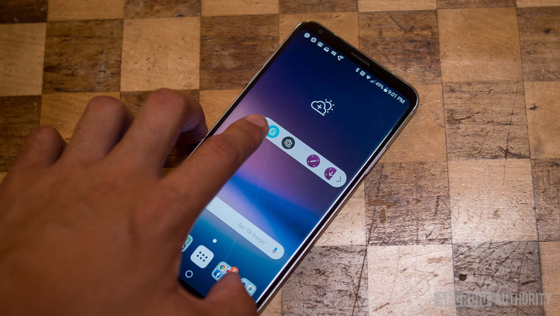
However, Sony’s technology was incredibly expensive, and the manufacturing technique was not commercially viable on a major scale. That hasn’t stopped companies investing in and improving microLED manufacturing techniques though, and industry mutterings suggest we are closing in on commercially viable production. This is shaping up to be the next arms race in display technology.
MicroLED tech explained
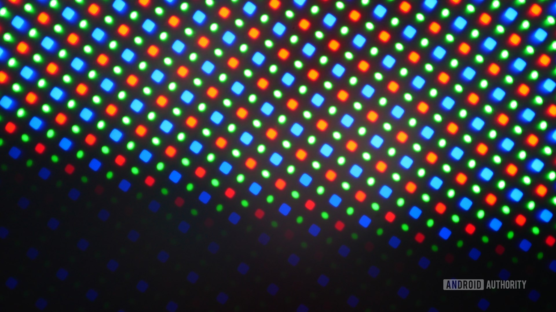
MicroLED shares a number of traits with OLED technology, making comparisons a little easier than LCD vs OLED debates. For starters, both have LED in their name, meaning that they’re both constructed from light emitting diodes. The two are “self-emitting” technologies, so each red, green, and blue sub-pixel produces its own light, unlike LCD, which requires a dedicated backlight. Therefore microLED displays will offer very high contrast ratios and deep blacks, just like OLED.
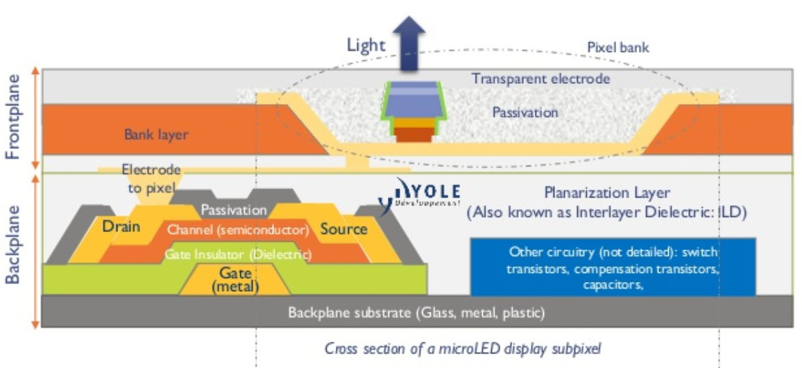
Where microLED differs from OLED is in the makeup of the LED materials. The O in OLED stands for organic and refers to the organic materials used in light producing part of the pixel stack. MicroLED technology changes this to an inorganic Gallium Nitride (GaN) material, which is typically found in regular LED lighting. This switch also reduces the need for a polarizing and encapsulation layer, making panels thinner. As a result, MicroLED components are tiny, hence the name, measuring less than 100 µm. That’s less than the width of a human hair.
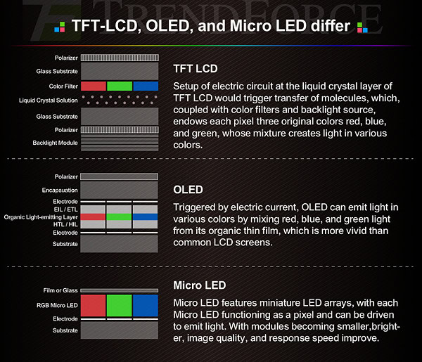
Another way of looking at this is that microLEDs are simply traditional LEDs shrunk down and placed into an array. The actually LED technology isn’t new, but manufacturing a panel array using such tiny components is the real difficulty. Conversely to other panel technologies, it’s actually easier to build small form factor microLED panels, such as smartwatches and smartphones. Scaling up to TV sizes is proving more difficult. However, squeezing very high resolutions into smartphone panel sizes is still tough to achieve, due to the high requirement for soldering accuracy.
MicroLED isn't reinventing display technology, instead, the unresolved problem for panel manufacturers is how to mass transfer and bond million of tiny LEDs.
The manufacturing problem
The unresolved problem for panel manufacturers is how to mass transfer and bond million of LEDs over to the control circuit panel. One potential solution sees the LEDs picked and placed into a larger array, to then be soldered to complete a display. The issue is that the accuracy of current pick and place manufacturing is ±34µm, which doesn’t meet the ±1.5µm accuracy requirements to place these tiny LED components.
Flip-chip technology isn’t without its problems either, even though it is currently the favored method for producing microLED panels. In this method, a wafer carrying the light emitting layer is flip-bonded onto the driver circuitry and then soldered. Unfortunately, this method is done one substrate at a time is therefore very slow. Investments are being made to improve yields, which suffer due to thermal mismatching and those pesky alignment accuracy issues.
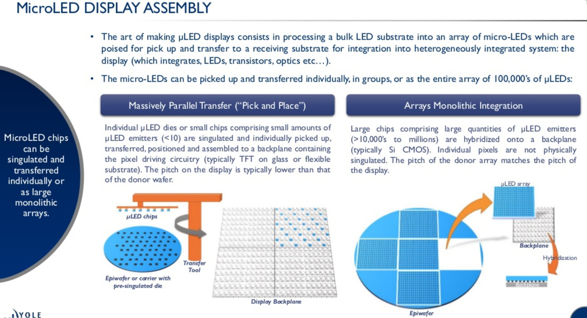
Alternative wafer production methods involve etching LED arrays for bonding to an IC. These etching methods avoid the accuracy problems of chip bonding, but improving the techniques to meet the small component sizes of microLEDs and the demand for high-resolution displays is expensive and difficult to implement. Manufacturing times are also very slow and refinement is still needed to improve yields.
JBD is developing a fabrication approach based on monolithic hybrid integration technology that should be better suited to small pitch LED for very high-density displays. JBD’s manufacturing method that bonds the LED to IC layer and then strips away the bonding material using a familiar semiconductor fabrication process, facilitating more cost-effective development. Taiwan’s PlayNitride and AUO are also working on LED chip technologies for this style of manufacturing, and talks have been taking place between them and Apple and Samsung.
We’ll have to see which method wins out and that might not be too long away. Production techniques are where major investments are being made in order to be the first to market with consumer panels.
Who’s working on microLED?
Much of the major news focused on microLED development suggests that Apple is looking to get into the display game with this technology for future phones. Rumors suggest that the company is developing its in-house microLED display technology to rid itself of reliance on Samsung’s OLED panels its iPhone range. In the long-term, such a move could save Apple significant component costs too, as OLED isn’t cheap. Apple has secured a number of patents for the technology, and the latest filing points to the use of a microchip driver bonded into a display substrate.
This would be a momentous step for Apple as its first in-house display technology. Although without any manufacturing equipment of its own, volume and yields for a major product launch would rely on the company outsourcing production. Apple had been in preliminary talks with PlayNitride regarding a partnership for manufacturing process technology, but this appears to have gone quiet. The price of a single 5-inch panel on its line was set to cost up to $300, making it significantly more expensive than premium OLED panels. Apple is also reported to be actively producing sample panels in conjunction with TSMC and visited AUO’s R&D center in Taiwan this year too, so is clearly assessing its options.

Major display players LG Display and Samsung are working in microLED, as is panel novice Apple.
We know that other major display manufacturers are eyeballing the technology for future products too. LG Display filed three brand names with the European Union Intellectual Property Office on March 20th 2018, listed as names XμLED, SμLED, and XLμLED. These names were trademarked specifically for smartphone devices. LG has also budged for production of its own huge 175-inch TV panel, following the unveiling of Samsung’s “The Wall” microLED set at CES.
Samsung had been pegged to buy PlayNitride for its own microLED panels, but instead, the company has been investing in the company’s chip production. Samsung also signed a deal with Chinese LED chip maker Sanan Optoelectronics in February 2018, paying $16.83 million to secure LED chips from the company. Chips from Sanan are being used in The Wall display.
As it stands out of the biggest players, Samsung and LG appear closest to launching commercial products, although even these giants appear reliant on technologies from other field specialists. Apple’s development schedule remains hidden behind closed doors, and Sony still has its surface mounted Crystal microLED technology too. Although who will be first to put the technology into a smartphone remains a wide-open race.
Pros and cons Vs. OLED
Despite the manufacturing hurdles, microLED technology is still worth pursuing because it offers up a number of improvements over OLED. The first is an improved brightness to power (lux/W) efficiency, meaning that the same panel brightness can be achieved for lower power. For comparison, power consumption can be 90 percent lower than LCD and up to 50 percent lower than OLED. This is potentially a major boon for portable technologies like smartphones, as it means much longer screen-on time. Alternatively, manufacturers can increase panel brightness without consuming additional power compared to current OLED and LCD, for better daylight viewing.
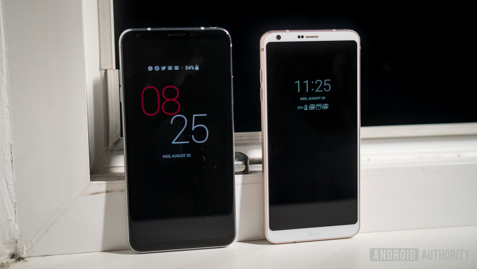
MicroLED displays will also offer a longer lifespan than current OLED panels. OLED burn-in is still a limited but real issue, due to the limited lifespan of the organic materials used to make the blue OLED. Micro-LEDs don’t exhibit the same problems and could even last longer than LCD displays before color shifting begins to occur.
The smaller microLED size also makes the prospect of higher resolution panels in a compact form factor, such as 4K or 8K smartphones or VR displays, more achievable. Speaking of VR, OLED panels already boasts very high response times in the µs (microsecond) range. This makes them ideal for virtual reality applications. However, microLED can reduce this down into ns (nanoseconds) or a thousand times faster.
MicroLED offers all of these benefits, while still retaining the high contrast ratio, wide color gamut, and potential use in flexible displays that we’ve come to associate with OLED. Unfortunately, these next-generation panels are also expected to be considerably more expensive, possibly three to four times higher than current LCD and OLED panels. This will undoubtedly fall in time, but it’s likely to discourage some immediate investments, especially as many panel manufacturers are still ramping up meaningful OLED production.
Final thoughts
MicroLED technology certainly looks promising, and there are plenty of upsides that are particularly well suited to mobile products. As OLED technology become increasingly common across more smartphone price points, high-end OEMs are almost certainly eyeing up microLED as their next-generation display technology.
Exactly when the first smartphone products will arrive remains an unknown for now. Samsung has kicked off its microLED production, but this is building its huge 146-inch TV. Apple has a growing portfolio of microLED patents that cover laptops and phones, and appears to be the most aggressive about pursuing this technology in the handset market.
However, there are also heavy investments being made into refining flexible OLED and bezel-less displays that might not make microLED the highest priority for every manufacturer. Even so, it seems likely that this technology will be the one the industry will eventually adopt in the longer term.
If you’re interested in the latest display technology advancements, be sure to check out what’s happening with Quantum Dots.