Affiliate links on Android Authority may earn us a commission. Learn more.
Why is Samsung's breakthrough in graphene research so promising for next generation electronics?
April 4, 2014

Samsung has announced some great news, they’ve made a breakthrough in graphene manufacturing. Graphene is that magical carbon substance that is destined to provide the world with next generation efficiency and flexibility for electronic components, such as flexible displays and wearable technology.
The Samsung partnership between the Samsung Advanced Institute of Technology (SAIT) and Sungkyunkwan University in South Korea, has figured out a way to produce large amounts of graphene using methods that could prove economical to full scale commercial manufacturing. As the cost to create graphene has been the largest barrier to its use in everyday electronics, this is a breakthrough that we should all be pleased about.
Why is this important?
As we demand more and more out of our everyday electronics like smartphones, tablets, and especially wearables like smartwatches, manufacturers face constant limitations of current building materials. Silicon is the predominant material utilized to build the individual electronic components within your favorite touchscreen enabled devices. As compared to silicon, graphene is said to have one hundred times the electron mobility. The use of graphene as a replacement for silicon would result in a faster, cooler and more efficient flow of electricity within our devices.
In addition to the electrical conductivity benefits of graphene, its physical makeup allows it to be extremely flexible and durable. In fact, it can stretch upwards of 20% of its initial length and is up to 300 times more durable than steel. As an added bonus, it has high heat conductivity as well. Basically, you would have to balance the weight of an elephant onto a pin-point to damage the one atom thick sheet of graphene.
“This is one of the most significant breakthroughs in graphene research in history. We expect this discovery to accelerate the commercialization of graphene, which could unlock the next era of consumer electronic technology.” - SAIT Labs
All of these characteristics make graphene the ideal material to build next generation flexible displays, flexible devices, vastly improved individual electronic components and much more.
What is graphene exactly?
Simply put, graphene is a one atom thick sheet of carbon atoms. Graphene measures in at 0.33nm, that’s almost one million times thinner than a human hair, 97.7% transparent and is made of carbon, which is far less expensive than the rare earth materials used in most current electronics manufacturing.
Although ideally suited to the production of flexible displays, graphene has been used to build ultra capacitors, faster transistors and processors and other nanotechnology. We took a good look at graphene, in relation to flexible displays, I encourage you to check that out here.
So, what exactly is Samsung’s breakthrough with graphene?
Samsung calls the new method “wafer-scale growth of single-crystal monolayer graphene on
reusable hydrogen-terminated germanium.”
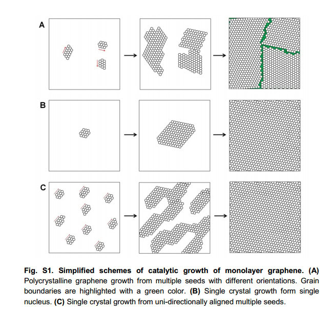
Traditionally, graphene has proven difficult, and therefore expensive, to produce. This has been due almost exclusively to the fact that producing graphene, especially in larger contiguous sheets, required a destructive process to transfer the material from its production environment over to the components it is being used to help build. The next biggest difficulty is actually growing graphene from individual ‘seeds,’ as they call them, into a single sheet.

In the science journal, Science Magazine and ScienceExpress, Samsung describes their new process of uniform growth of single-crystal graphene over wafer-scale areas. They focus on how graphene could be made commercially viable through their new etch-free dry transfer technique that allows them to re-use the production environment for further graphene growth. Previous methods required a liquid based transfer of the graphene, but now, the germanium substrate layer that graphene is produced on top of can be re-used for continual growth of graphene, instead of being destroyed in the transfer process. Here is the abstract introduction to the science journal, just for a good read.
ABSTRACT The uniform growth of single-crystal graphene over wafer-scale areas remains a challenge in the commercial-level manufacturability of various electronic, photonic, mechanical, and other devices based on graphene. Here, we describe wafer-scale growth of wrinkle-free single-crystal monolayer graphene on silicon wafer using a hydrogen-terminated germanium buffer layer. The anisotropic twofold symmetry of the germanium (110) surface allowed unidirectional alignment of multiple seeds, which were merged to uniform single-crystal graphene with predefined orientation. Furthermore, the weak interaction between graphene and underlying hydrogen-terminated germanium surface enabled the facile etch-free dry transfer of graphene and the recycling of the germanium substrate for continual graphene growth.The final result is larger and far more efficient production of graphene sheets. With this technique, Samsung could enable the use of graphene in our commercially available everyday electronics. Stronger, more energy and heat efficient flexible touchscreens and devices are all possible.
What’s next?
Companies like Nokia, which invested $1.36 billion into graphene research last year, and schools like the University of Manchester, with £50 million from the UK and EU governments, have nearly ten thousand patent applications filed for graphene research. Even then, graphene requires a lot more innovation before it can be produced economically at scale.
Samsung’s breakthrough in graphene production helps overcome one of the major hurdles that has been preventing widespread adoption of graphene in electronics manufacturing. However, it is not mentioned what overall cost savings are expected, nor at what scale the new techniques will allow graphene to be produced. We’ll be anxiously awaiting the next steps that Samsung takes to bring graphene to the market.
So, Samsung Fingers – April Fools’ Day joke, or product teaser?